Indium tin oxide is a transparent conducting oxide (TCO), designed for conducting electricity without sacrificing visibility. Its optical transparency, durability, conductivity and relative cost-effectiveness make it a great choice for dozens of applications. Touchscreens, solar cells, television and computer displays, and other products all feature ITO coatings.
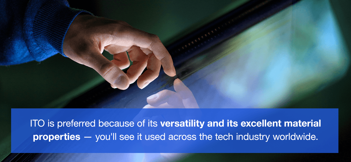
ITO is preferred because of its versatility and its excellent material properties — you'll see it used across the tech industry worldwide.
Understanding ITO Properties
ITO's unique properties make it an extremely versatile material. Its conductivity, refractive index and thermal properties offer an ideal combination for many operations. These are the main properties of ITO that make it so useful for different industries:
- Conductivity: One of ITO's most notable material properties is its conductivity. ITO has free electrons, which give it its high conductivity. This property makes ITO an excellent choice for applications involving transparent conductive coatings, like solar cells, smart windows, LCDs and touchscreens.
- Refractive index: A material's refractive index tells you how much light gets bent or refracted when it travels through the material from elsewhere. ITO's refractive index is relatively low compared to other transparent conductive materials like metals. This low refractive index helps minimize light reflection, enhance transparency and reduce other optical losses. ITO-coated surfaces look clearer and provide better visibility thanks to these conditions.
- Thermal properties: ITO also has effective thermal properties. It has a low thermal expansion coefficient and high thermal stability, making it perfect for fluctuating temperatures. It will maintain performance even when its environment changes temperatures rapidly. Additionally, ITO is a highly efficient heat dissipater. This feature prevents overheating, making devices with ITO coatings last longer and perform more reliably.

ITO Applications
ITO's conductive, refractive and thermal properties make it ideal for solar and touchscreen applications. These areas require material to work reliably under high heat conditions without losing efficiency. Additionally, these applications need a coating that is transparent enough to allow the device to function correctly.
Solar Cells
ITO is crucial for solar cells. It's used as a TCO that lets sunlight pass through to the solar cell, encouraging electricity collection. Its high conductivity helps with efficient electron transport, improving electrical energy extraction. Additionally, ITO's transparency lets sunlight travel through the cell instead of getting absorbed, which keeps the solar cell efficient. With better energy extraction and minimal sunlight absorption, the solar cell can continue to harvest light.
Touch Screen Technologies
ITO is also used in glass coatings for touchscreen devices like smartphones, tablets and other displays. ITO is conductive and transparent, making it ideal for touch-sensitive surfaces that need to track user touch inputs. ITO can detect the electrical resistance created by your fingers on the touch screen, helping with more precise tracking. Further, ITO is durable and scratch-resistant. These qualities make it perfect for ensuring touch screens have longer life spans.
Innovations in ITO Coating Techniques
There are several ways to apply ITO coatings. Different techniques provide different benefits, and the exact technique used might depend on the end goal and the coating company.
Sputtering vs. Evaporation Methods
Sputtering and evaporation are the two main methods used in ITO coating.
- Sputtering: Sputtering bombards the ITO material with ions, ejecting ITO atoms onto the desired surface in an even coating. Driving the ITO atoms into the material creates an extremely strong bond — you get a permanent coating instead of a layer of ITO on top of your material. Sputtering gives you precise control over your material's thickness and uniformity, creating accurate, even coatings on a range of materials.
- Evaporation: The evaporation method involves heating the ITO in a vacuum until it vaporizes. After vaporizing, ITO gets condensed onto a substrate. This condensation of the vaporized ITO turns it into a thin film. Evaporation works well for smaller-area applications, but sputtering is better for large-area deposition. Sputtering is the preferred method in many situations, though evaporation still provides excellent electrical properties.
ITO Recycling Methods
Recycling is a great way to use ITO sustainably. With recycling, operations can reuse ITO for other purposes, reducing waste and maximizing product efficiency. Here are some of the potential recycling methods used for ITO:
- Separation: Used electronics like tablets and phones with ITO-coated screens are taken apart, and the glass is collected. The ITO-coated glass is treated to separate the ITO layer and remove impurities. Finally, operations will purify the ITO so it can be used again.
- Reclaiming scraps: Excess ITO scrap material gets collected and melted down. This melted-down ITO can then be used in new coatings.
- Waste reduction: Operations might also focus on sustainability by reducing total ITO usage during production. Designing products with recyclability in mind and cutting waste during production helps make the above processes easier. Additionally, reusing old electronics or taking them to recycling centers helps prevent landfill waste.
Exploring ITO Alternatives
ITO is a highly versatile, useful material. However, steps are being taken to find more sustainable, cost-effective alternatives. While ITO will likely always be used in some capacity, finding alternatives can reduce the cost burden on consumers and manufacturers and help protect the planet. Check out these materials that might make effective ITO alternatives:
- Graphene: Graphene is a form of carbon — its name comes from “graphite.” Graphene is a thin, hexagonal shape made from carbon atoms that could take the role of ITO in some applications. It has excellent transparency and electrical conductivity, but it's expensive to produce. Graphene also has a low production yield, still making it slightly undesirable as an ITO replacement. It could potentially work well in touchscreens and solar cells.
- Silver nanowires: Silver nanowires are a more environmentally friendly alternative to ITO. They can also form transparent and conductive films and offer excellent flexibility. However, they have less temperature stability than ITO, making them less suitable for solar cells and device screens.
- PEDOT: Poly(3, 4-ethylenedioxythiophene), or PEDOT, has been a non-traditional alternative for ITO in some situations. It has high electrical conductivity and good optical transparency, making it a potential candidate for device screens and solar cells. It's also highly flexible and more environmentally friendly than ITO. However, PEDOT does not quite reach ITO's sheet resistance and ultraviolet stability standards. More expensive techniques would need to be used to make PEDOT match ITO.
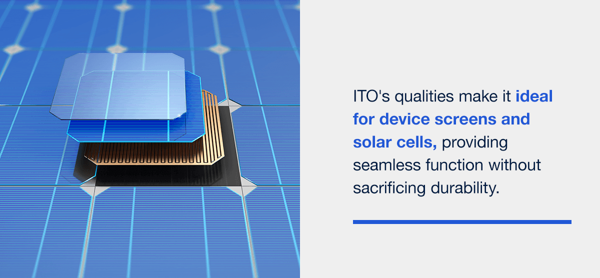
Currently, ITO's excellent performance and widespread use have made it unmatchable in its performance sectors. With future advancements, a material could compete with ITO. ITO's qualities make it ideal for device screens and solar cells, providing seamless function without sacrificing durability.
Connect With MSE Supplies
MSE Supplies is a leading supplier of ITO coated glass substrates and ITO coated PET films with a worldwide customer base. Many well known labs around the world have been using our ITO products in their research and product development projects. Both standard and customized (patterned) ITO substrates are available from MSE Supplies. Contact us today to discuss your project requirements.