
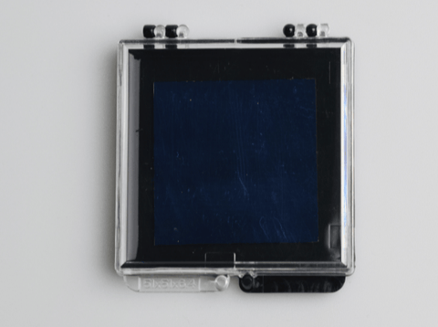
MSE PRO Monolayer Hexagonal Boron Nitride Film (hBN) on SiO2/Si Substrate
SKU: ME0650
MSE PRO™ Monolayer Hexagonal Boron Nitride Film (hBN) on SiO2/Si Substrate
Hexagonal boron nitride (h-BN), which is also called “white graphene”, has gained special attention for its various outstanding properties including high thermal conductivity, a low dielectric constant, chemical inertness and high mechanical strength. Monolayer hexagonal boron nitride (h-BN), a honeycomb lattice with strong ionic bonding of boron and nitrogen atoms, is the thinnest insulating nanomaterial with an electrical band gap of 5.9 eV. It has a wide range of applications from protective coating, thermal interface material, transparent membrane and deep UV optoelectronic devices. Furthermore, due to its very small lattice mismatch (~2%) with graphene, atomic-scale smoothness and free of dangling bonds, the h-BN has been regarded as the perfect substrate for graphene device applications.
- Substrate: SiO2/Si
- Shape: Rectangle
- Size: 1"x1" (SKU# ME0650), 1"x2" (SKU# ME0651) and 2"x2" (SKU# ME0652)
- Grain Size :> 4um
- Coverage : 100%
- SiO2 Thickness : 300nm
- Si Thickness: 500um
References:
1. Monolayer hexagonal boron nitride films with large domain size and clean interface for enhancing the mobility of graphene‐based field‐effect transistors. Advanced materials 26, no. 10 (2014): 1559-1564.