Customized Germanium Tin (GeSn) Epitaxial Wafer On Silicon Substrate
To better serve you, we would like to discuss your specific requirement, Please Contact Us for a quote.
Customized Germanium Tin (GeSn) epitaxial wafers can be provided by MSE Supplies to meet your specific project requirements. The Silicon (Si) substrate are available from 4 inch up to 8 inch. The epitaxial GeSn layer are grown with the CVD process and is possible with electrically active doping of P-type and N-type. The epitaxial layer thickness depending on configurations.
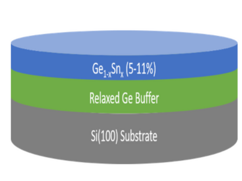
Germanium Tin (GeSn) alloys can be grown through Chemical Vapor Deposition (CVD) or Molecular Beam Epitaxy (MBE) process. The differences between CVD and MBE are CVD is the most common growth method in the industry due to much lower cost; however MBE can be more accurate. No matter what method used, both are quite hard to realize as the solubility of Tin (Sn) in Germanium (Ge) is low. During the epitaxy process, GeSn is grown on relaxed Ge buffer. The surface roughness typically increase when Sn content gets higher (RMS of < 2nm is still possible). The advantages of GeSn epitaxial wafers are the following. Ge is indirect a band gap material. However, when incorporating Sn into Ge at around 9%, it becomes direct band gap semiconductor. Becoming direct band gap means the recombination process is more efficient, which can be used in optical devices. Furthermore, the researchers at multiple institution including CEA Leti, University of Leeds have discovered that the emission/absorption limit of GeSn alloys can be extended up to 0.35eV, making the alloys one of the ideal candidates for optoelectronics in the mid-infrared region. It is widely used in various communication applications, including but not limited to infrared light emitting diodes (IR LEDs), laser and detectors.
MSE Supplies offers epitaxy services on various substrate. Please contact us if you need customization or bulk order.
Capability:
| Substrate | Silicon Wafer |
| Wafer Size | 4 inch / 6 inch / 8 inch |
| Sn Content | X% (Typically X=5~11) |
| Ge Content | (1-X)% |
| Ge Buffer Thickness | 600~1000 nm |
| Ge1-xSnx Epi Layer | strained / relaxed |
| Ge1-xSnx Epi Layer Thickness | thickness depending on configurations |
References:
Price:
MSE Supplies offers the best price on the market for high quality GeSn epitaxial wafers up to eight (8) inch diameter. Our price matching policy guarantees you the best price for the GeSn epitaxial wafers with comparable specifications. CONTACT US today to get your quote.
Customization:
Customized Germanium Tin (GeSn) epitaxial wafers can be provided by MSE Supplies to meet your specific project requirements. The Silicon (Si) substrate are available from 4 inch up to 8 inch. The epitaxial GeSn layer are grown with the CVD process and is possible with electrically active doping of P-type and N-type. The epitaxial layer thickness depending on configurations
