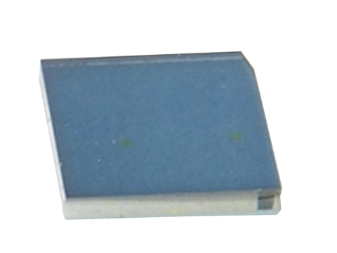
Diamond Epitaxial Wafer for Diodes
SKU: WA1871
Diamond Epitaxial Wafer for Diodes
MSE Supplies offers Diamond Epitaxial Wafer with either p-type or n-type doping for various applications. It has extremely high current density and voltage compared to the widely used silicon. The devices made with diamond can operate in harsh environments like high temperature and radiation. These wafers could also easily handle higher voltage and reduce energy losses by a factor of 10 compared to silicon. Diamond has been investigated as the potential material for the compact power converters for automobiles. It can be used in various applications, including power electronics, nuclear, spatial, quantum, etc.
Specification:
| Diamond Substrate | |
| Dimension | 4 mm x 4 mm |
| Thickness | 0.5 mm |
| Orientation | <100> |
| Type | Ib |
| Epi Layer 1 | |
| Thickness | 2 μm (1 kV) or 6 μm (3 kV) |
| Type | intrinsic diamond |
| Epi Layer 2 | |
| Thickness | ~500 nm |
| Type | p++ conductive diamond |
*Please note that actual products might be different from the picture.
Customization:
Customized Diamond Epitaxial Wafer can be made to meet customer's particular requirements and specifications. Please contact our team to discuss your requirements and get a quote.
References:
