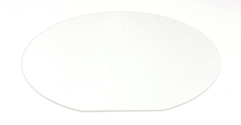
MSE PRO SiO2 Silica Quartz Single Crystal Wafers and Substrates
Single crystal quartz wafers are ideal for use as substrates for thin film deposition and are also suitable for many optical applications. Quartz single crystal wafers and substrates are also used as microwave filters in wireless communication.
MSE Supplies offers both standard and custom-made quartz wafers and substrates.
|
Typical Material Properties |
|
|
Purity |
Optical grade: 99.99% |
|
Crystal Structure and lattice parameters |
Hexagonal a= 4.914 Å c = 5.405 Å |
|
Growth Method |
Hydrothermal method |
|
Hardness |
7.0 Mohs |
|
Density |
2.684 g/cm3 |
|
Melt Point |
1610 deg C (phase transition point: 573.1 °C) |
|
Specific heat |
0.18 cal/g |
|
Thermoelectric Constant |
1200 mV / °C @ 300 °C |
|
Thermal conductivity |
0.0033 cal/cm/ °C |
|
Thermal expansion coefficient, (CTE) (x10^-6/ K) |
perpendicular to Z axis: 13.71 parallel to Z axis: 7.48 |
|
Refractive Index |
1.544 |
|
Q value Acoustic velocity, SAW Frequency constant, BAW Piezoelectric coupling , |
1.8 x 10^6 minimum 3160 ( m/sec ) 1661 ( kHz/mm ) K2 (%) BAW: 0.65 SAW: 0.14 |
|
Inclusion |
IEC Grade II |
|
Standard Quartz Wafer Specifications |
|
|
Quartz Crystal Orientation |
Y, X, Z, AT or ST cut. The cut angle can be rotated to any value in the in the range of 30 deg ~ 42.75 deg upon request.  Primary flat: orientation specified by customer Secondary Flat: orientation specified by customer. Seed: located in the center with width < 5mm and height > 66mm |
|
Polished surface |
Epi-ready polished on one side or two sides to Ra < 1 nm Working Area: Wafer diameter minus 3 mm (edge exclusion) BOW: < 20 um for 3" wafer and 30 um for 4" wafer No chips out on the working area. At the edge, chip width < 0.5 mm Pits and scratches: < 3 per wafer or < 20 per 100 wafers |
|
Standard Thickness |
0.5 mm +/- 0.05 mm TTV < 5 µm |
|
Standard Diameter |
dia. 2 inch (50.8mm ) diam. 3 inch (76.2mm) dia. 4 inch (100mm) +/-0.2 mm Primary Flat: 22 +/- 1.5 mm (dia. 3¨ ) 32 +/- 3.0 mm ( dia. 4¨ ) Secondary Flat: 10 mm +/-1.5 mm |
|
Production Capacity |
>1,000 wafers per month |
Customized products are available upon request.
