MSE Supplies Products
Advanced Materials
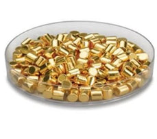
MSE Supplies' extensive portfolio of advanced materials are uniquely suited to meet the requirements of today's most challenging applications and innovations. We offer various advanced materials including sputtering targets, battery materials and nano materials for battery research and development, semiconductors, biosensors, etc.


Laboratory Equipment
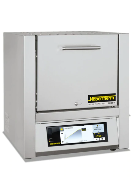
MSE Supplies is a leading supplier of laboratory equipment in the US. Our selection of lab equipment consists of the best quality from many leading brands. We offer battery manufacturing equipment from electrode preparation to battery sealing and testing. Besides, we have various lab equipment such as sputter coaters, planetary ball mills, lab furnaces, etc.


Lab Supplies
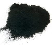
When it comes to Lab Supplies, you can count on MSE Supplies. Supplies and solutions for every industry, plus easy ordering and professional customer support. We offer various supplies and consumables for battery research including current collectors, binders, cathode and anode materials, solid-state electrolytes, etc. We also offer lab supplies for semiconductors and biotech research.


Services
MSE Analytical Services department provides high-value materials characterization analytical services with a large number of advanced analytical instruments available to measure your samples. We offer power analysis (e.g. powder XRD, laser particle size analysis), surface characterization (e.g. AFM, XPS, SEM), pore structure tests such as BET characterization and mercury porosimetry, and even ICP-MS/ICP-OES to identify chemical compositions for samples. Accurate, Efficient, and Affordable materials analytical services with the guaranteed best value.

Other Products
MSE Supplies is your source for innovative, indispensable lab equipment, lab supplies, and analytical services. View our wide selection of products for scientific research and production both standard and custom-made for you.
