MSE PRO 2 inch Si-doped N-type GaN 4.5 um Gallium Nitride Template on Sapphire (0001)
Features for 2 in Si-doped N-type 4.5 um Gallium Nitride Template on Sapphire, SSP or DSP
Part No: WA0204 for SSP sapphire substrate, WA0223 for DSP sapphire substrate- Conductivity type: N-Type (Si-doped)
- Sapphire Substrate Polish: Single side polish (SSP) or double side polish (DSP)
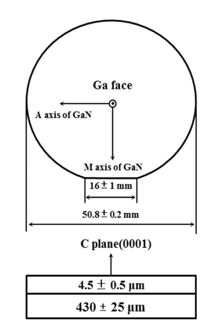
- Dimension: 50.8 mm +/- 0.2 mm (2 inch diameter)
- GaN Thickness: 4.5 +/- 0.5 um
- Usable area: >90%
- Orientation of GaN: C plane (0001) off angle toward A-axis 0.2 ± 0.1 deg
- Orientation Flat of GaN: (1-100) +/- 0.2 deg, length 16.0 +/- 1.0 mm
- Total Thickness Variation: < 15 um
- Resistivity (300K): < 0.05 Ohm-cm
- Dislocation Density: < 5x108 cm-2
- Carrier concentration (~ doping concentration): > 1x1018 cm-3
- Mobility > 200 cm2/V-s
- Surface AFM RMS: < 0.5 nm with CMP polishing, epi-ready
- Sapphire substrate thickness: 430 +/- 25 um
- Orientation of sapphire substrate: C plane (0001) off angle toward M-axis 0.2 ± 0.1 deg
- Orientation Flat of sapphire: (11-20) 0 ± 0.2 deg, length 16.0 +/- 1.0 mm
- Structure: GaN/Sapphire (0001)
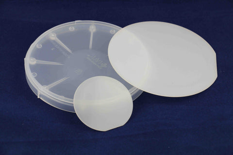
- Package: packaged in a clean room environment, in cassettes or single wafer containers.
Related References:
1. Si- and Ge-Doped GaN Films Grown with GaN Buffer Layers
https://doi.org/10.1143/JJAP.31.2883
2. Band-gap re-normalization and band filling in Si-doped GaN films studied by photoluminescence spectroscopy
https://doi.org/10.1063/1.371377
3. The role of dislocation scattering in n-type GaN films
https://doi.org/10.1063/1.122012
4. Activation energies of Si donors in GaN
https://doi.org/10.1063/1.115805
The electronic properties of Si donors in heteroepitaxial layers of GaN were investigated. The n-type GaN layers were grown by metal organic chemical vapor deposition and either intentionally doped with Si or unintentionally doped. The samples were evaluated by variable temperature Hall effect measurements and photoluminescence (PL) spectroscopy. For both types of samples the n¨«type conductivity was found to be dominated by a donor with an activation energy between 12 and 17 meV. This donor is attributed to Si atoms substituting for Ga in the GaN lattice (SiGa). The range of activation energies is due to different levels of donor concentrations and acceptor compensation in our samples. The assignment of a PL signature to a donor acceptor pair recombination involving the Si donor level as the initial state of the radiative transition yields the position of the optical Si donor level in the GaN band gap at uEc(22+/-4) meV. A deeper donor level is also present in our GaN material with an activation energy of 34 meV which is tentatively assigned to oxygen donors substituting for nitrogen (ON).