


MSE PRO 8 inch Schott Borofloat 33 Glass Wafer, 700 um thick, DSP
Couldn't load pickup availability

Still have questions? Ask our experts!
MSE PRO 8 inch Schott Borofloat 33 Glass Wafer, 700 um thick, DSP
Introduction
Schott Borofloat® 33 is a high-quality borosilicate glass known for its outstanding properties, making it suitable for various applications. BF33 is Manufactured using the advanced Microfloat process. It is a transparent, colorless glass features excellent optical quality, a smooth surface, and high flatness.
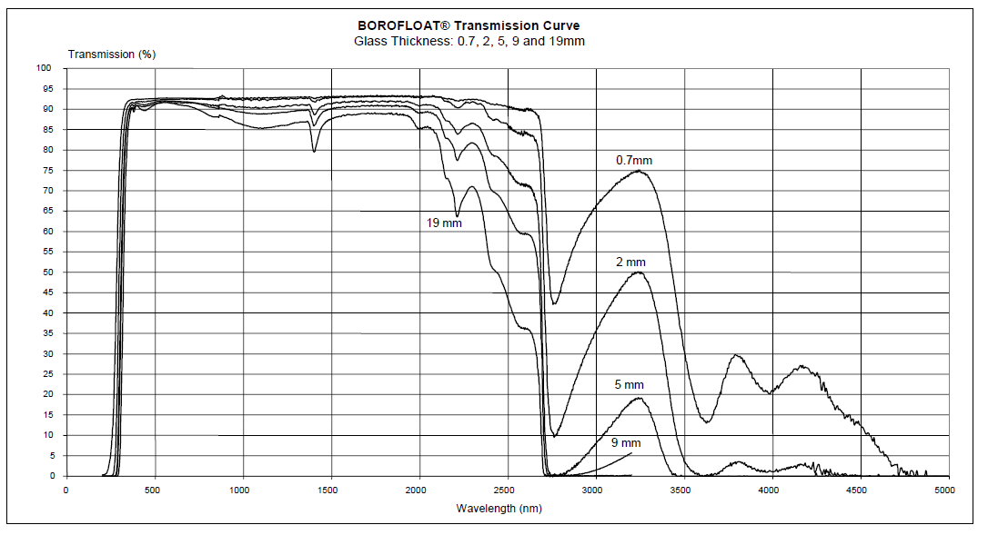
Borofloat 33 achieves a transmission rate exceeding 90% and has minimal fluorescence across the light spectrum. These qualities make it ideal for optics, optoelectronics, and photonics. Its low thermal expansion and high thermal shock resistance allow it to withstand temperatures up to 450°C, ensuring stability in temperature-sensitive applications.
This glass also resists water, acids, and alkalis, making it well-suited for the chemical industry and analytical technology. Notably, Borofloat33 is widely used in silicon wafer anodic bonding, providing excellent compatibility with silicon substrates for microelectronics and biotechnology.
Key Properties
- Exceptional Optical Quality – >90% transmission in the visible spectrum with low absorption, excellent homogeneity, low birefringence, and high imaging accuracy.
- Excellent Surface Flatness – Microfloat process ensures mirror-like surface finish, low roughness, high parallelism, and uniform thickness for precision applications.
- Low Thermal Expansion – Its coefficient of thermal expansion closely matches silicon, reducing thermal stress and enabling high dimensional stability and reliable bonding.
- High Thermal Shock Resistance – Withstands rapid temperature changes and operates up to ~450°C, suitable for vacuum and semiconductor processing environments.
- Outstanding Chemical Resistance – Resistant to water, humidity, acids, organic solvents, and many alkaline environments for long-term durability.

Chemical Composition of Schott Borofloat Borosilicate Glass
Key Applications
- MEMS Manufacturing – Used as a substrate for pressure sensors, accelerometers, MEMS microphones, optical MEMS, and inertial sensors due to silicon compatibility.
- Silicon Anodic Bonding – Ideal for MEMS packaging, microfluidic chips, biomedical devices, and wafer-level packaging with strong bonding and high reliability.
- Microfluidics – Suitable for lab-on-a-chip systems, including cell analysis, DNA sequencing, PCR devices, chemical reactors, and diagnostics.
- Optical Components – Applied in optical windows, filters, beam splitters, mirrors, lens substrates, and camera protection windows.
- Photonics – Supports optical sensors, waveguides, photonic integrated devices, laser systems, and fiber optic components.
- Semiconductor Industry – Used for wafer carriers, temporary bonding substrates, packaging lids, cover glass, and inspection windows.
- Biomedical Devices – Ideal for biochips, DNA microarrays, medical sensors, diagnostic equipment, and cell culture devices.
- Analytical Instruments – Widely used in spectroscopy, chromatography, optical analysis, precision measurement, and scientific instruments.
Specifications
| Diameter/size (or square) | 200 mm |
| Tolerance (±) | 0.2 mm |
| Thickness | 700 µm |
| Tolerance (±) | 25 µm |
| TTV | < 3 µm |
| Bow | ±40 µm |
| Warp | ≤ 50 µm |
| Edge Rounding | SEMI M1.2 / IEC 62276 compliant |
| Surface Type | DSP |
| Polished side Ra | ≤ 1 nm |
*The photo is for reference only. The appearance might be different due to difference in dimensions.
Custom made fused silica and glass substrates are available upon request. Please contact us for a quote for bulk orders and customizations.