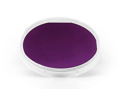
Silicon/Silicon Dioxide (Si/SiO2) Wet Thermal Oxide Silicon Wafer and Substrates, Prime Grade
Thermal oxide (silicon dioxide, SiO2) layer is formed on silicon wafer surface at an elevated temperature in the presence of an oxidant. This process is commonly referred to as a thermal oxidation process. The SiO2 thermal oxide thin film is normally grown in a horizontal tube furnace, at temperature range from 900°C ~ 1200°C.
Silicon/silicon dioxide (Si/SiO2) thermal oxide wafers and substrates are widely used for FET substrates, surface microscopy analysis, ellipsometry measurements and X-ray studies. MSE Supplies also offers monolayer graphene film on Si/SiO2 substrate. (10mm x 10mm, 1 inch x 1 inch, and more...)
We can offer a variety of choices for customization. Please contact us at sales@msesupplies.com for your requirements of customized products.
MSE Supplies offers the following choices:
- Type of silicon wafer: N or P type
- Silicon wafer doping: un-doped, P-doped or B-doped
-
SiO2 thickness: 300~500 nm. The standard thickness is 300 nm.
- Electrical resistivity: un-doped (>1000 Ωcm), P or B doped (10-3~104 Ωcm)
- Crystal orientations: (100), (111) and (110)
- Substrate sizes: 10x10 mm, 15x15 mm, 2", 3", 4" or customized
- Thickness: 0.3~0.5 mm, 1.0 mm or customized
- Surface polishing: Single Side Polished (SSP) or Double Side Polished (DSP)
|
Properties |
|
| Crystal Structure of Si | Face-centered cubic |
| Melting Point | 1410 ℃ |
| Density | 2.4 g/cm3 |
| SiO2 Thermal Oxide Film Thickness | 300 nm |
| EPD | ≤100∕cm2 |
| Oxygen Content | ≤1~1.8 x 10^18 atoms/cm3 |
| Carbon Content | ≤5 x 10^16 atoms/cm3 |
| Size Tolerance | <±0.1mm |
| Thickness Tolerance | <±0.015mm or <±0.005mm upon request |
| Wafer Orientation Precision | ±0.5° |
| Edge Orientation Precision | 2° (1° if requested) |
| Packing | Packed with class 100 clean wafer case or bag in a class 1000 cleanroom |
